Wafer Level & Fan Out
Packaging Technology

Delivering topnotch performance and speed while maintaining a small, thin, and cost-effective form factor.

Designed for Speed and Efficiency

Today’s consumers seek powerful, multi-functional electronic devices that combine exceptional performance and speed with a compact, lightweight, and cost-effective design. These demands pose significant technological and manufacturing challenges for semiconductor companies. As a global leader in advanced packaging solutions, STATS ChipPAC delivers state-of-the-art wafer-level technology platforms that not only address these challenges but also set new benchmarks in electronic device innovation.

Comprehensive Wafer Level
Technology Solutions

STATS ChipPAC provides an industry-leading portfolio of wafer level packaging solutions tailored to meet diverse application needs. Our advanced technology platforms include:

Fan-in Wafer Level Packaging (FIWLP)

Designed for compact and cost-sensitive devices, FIWLP enhances performance while minimizing footprint.

Fan-out Wafer Level Packaging (FOWLP)

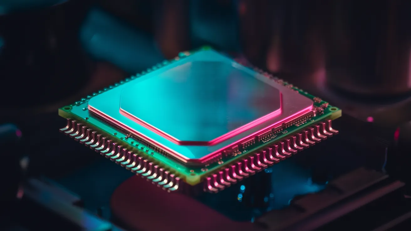
A revolutionary packaging solution enabling higher performance and functionality with reduced package size and improved thermal and electrical performance.

Integrated Passive Devices (IPD)

Compact integration of passive components to enhance performance and functionality in RF and mixed-signal applications.

Through Silicon Via (TSV)

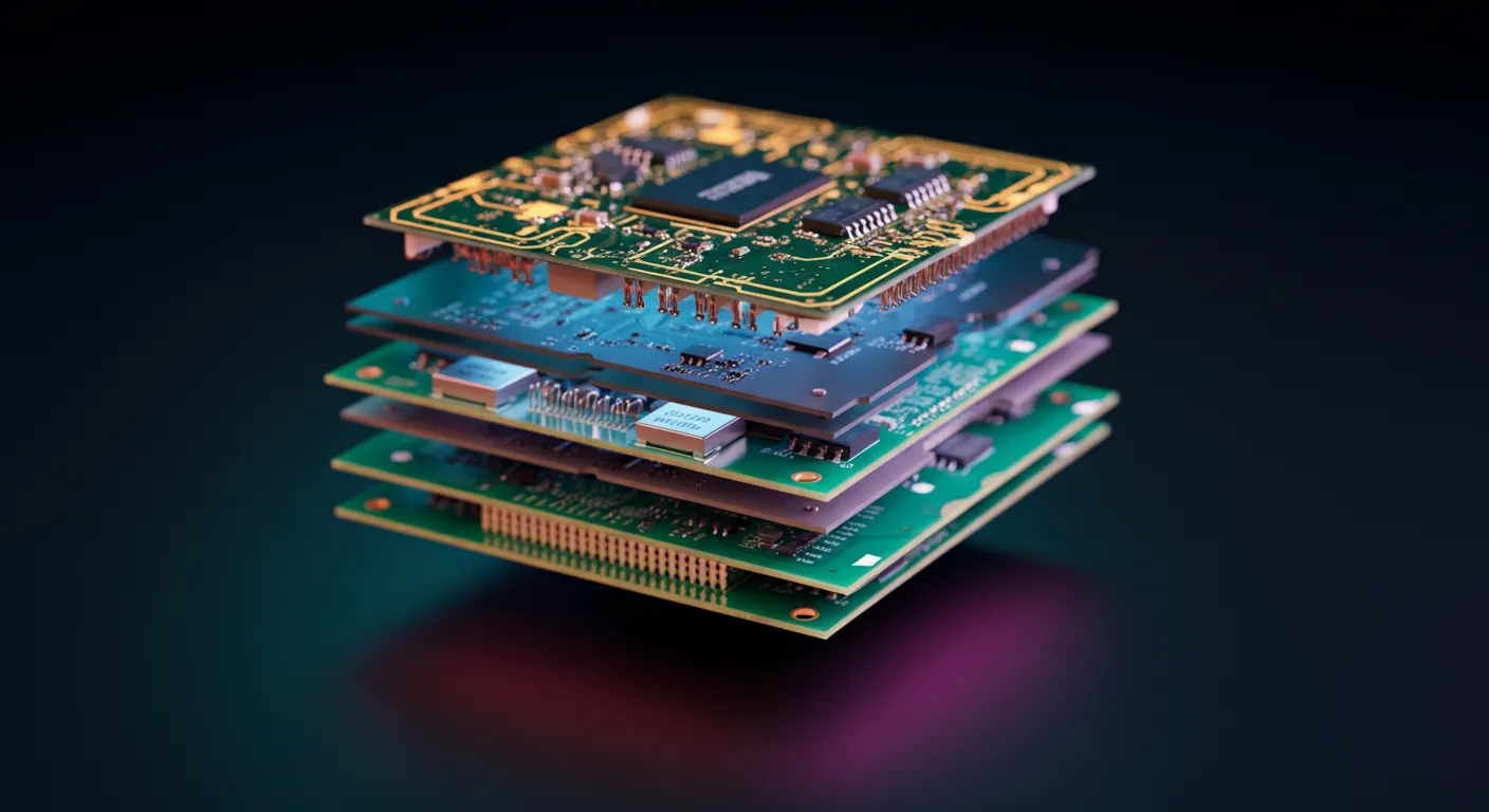
Advanced 3D interconnect technology that delivers high bandwidth, low latency, and superior power efficiency.

Encapsulated Chip Package (ECP)

Protection and reliability for electronic components with encapsulated solutions.

Radio Frequency Identification (RFID)

Pioneering solutions for seamless connectivity and secure data transmission.

Technologies That Drive Your Innovation

Find out how else we can help your organization.

Explore All Technologies

Find out how else we can help your organization.

2.5/3D Integration

Integrate multiple components into a single compact package.

System-in-Package

Integrate multiple components into a single compact package.

Flip Chip Packaging Technology

Integrate multiple components into a single compact package.

Superior Memory Packaging

Integrate multiple components into a single compact package.

Downloads

Embedded Wafer Level Ball Grid Array (eWLB)
Innovations in Wafer Level Technology
WLCSP - Wafer-Level Chip Scale Package
28nm Chip-to-Package Interaction in Large Size eWLB...
Challenges and Improvement of Reliability in Advance Wafer Level...
eWLCSPTM - Encapsulated Wafer-Level Chip Scale...
Reliability of eWLB for Automotive Radar
3D Integrated eWLB FOWLP Technology for PiP and...
Advanced 3D eWLB-PoP Technology