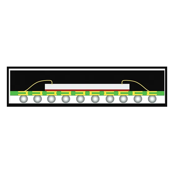
Advanced packaging for the 5G era.

High-frequency, high-speed, low-latency, and multi-channel demands are reshaping IC packaging in the 5G era. STATS ChipPAC offers a full suite of advanced packaging and testing solutions, including 2.5D/3D, wafer-level packaging, and system-in-package (SiP), supported by collaborative design, simulation, and automated quality control.

Our integration capabilities include high-density SMT, laser-assisted bonding (LAB), double-sided molding SiP, and EMI shielding, enabling scalable production for RF front-end modules, millimeter-wave antennae AiP, and other high-performance 5G components.

Packaging & Technology Portfolio

Where proven solutions meet evolving demands.

HPC & AI

AP, DSP, FPGA, ASIC, MCU, …
fcBGA-H-SiP
2.5D HDFO
fcCSP
PoP

Connectivity

Wearables, WiFi, BLE, NB IoT
LGA
BGA
DSM SiP

RF

PA, RFFE Module, mmWave, AiP
Hybrid SiP
DSM SiP
AiP

Sensors

Motion, Pressure, Optical MEMS Sensors
Hybrid LF / HFBP
Cavity LF
Exposed Die / Glass

Core Capabilities

  • SiP, PoP, AiP, and XDFOI® packaging
  • FC, WB, and SMT processes
  • Thermal management and final test services

Supports 008004 devices, 45 µm spacing, and ±15 µm SMT accuracy

  • High-speed EMI shielding options
  • Single-sided, double-sided, and 3D SiP
  • Turnkey wireless test solutions

Packaging solutions for electromagnetic, current, pressure, temperature, humidity, optical, inertial, and other sensor types

Application Advantages

High-Performance Computing (HPC) and AI
Connectivity
Radio Frequency (RF)
Sensors