2.5/3D Integration

Driven by the demand for mobile data, STATS ChipPac advances beyond traditional packaging with 2.5D/3D designs using wafer-level, flip chip, and Through-Silicon Via technologies.

Comprehensive Solutions for Complex Requirements

STATS ChipPac’s expertise in advanced packaging, wafer-level integration, and silicon-level interconnects ensures that customers receive reliable, scalable, and cost-effective solutions. A focus on continuous innovation and stringent quality standards makes us the trusted partner for advanced integration technologies by industry leaders worldwide.

Double-sided molding

the technology effectively reduces the package size, shortens the connection of multiple dies and passive devices, reduces resistance, and improves the electrical performance of the system.

EMI shielding

JCET uses back metallization technology to effectively improve thermal conductivity and EMI shielding.

Laser-assisted bonding
(LAB)

the technology is able to overcome traditional reflow bonding problems, such as CTE mismatch, high warpage, high thermal mechanical stress, and other reliability problems.

Get Advanced Stacked Package Solutions with Package Level Integration

Package-level integration focuses on stacking and interconnecting multiple chips using wire bonds or flip chip processes. This enables higher performance and space efficiency while supporting various configurations:

Stacked Die (SD) Packages

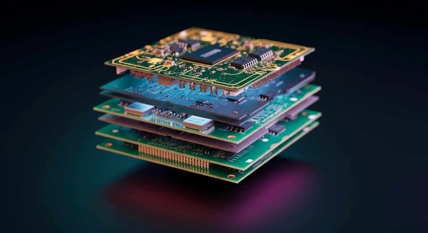
Utilises wire bond and flip chip connections to stack bare dies in standard packages. Common configurations include FBGA-SD, FLGA-SD, PBGA-SD, QFP-SD, and TSOP-SD.

Package-on-Package (PoP)

Stacks fully tested memory and logic packages, simplifying IC technology integration. Options include Bare Die PoP, Molded Laser PoP, and PoP-MLP-ED for enhanced flexibility.

Package-in-Package (PiP)

Combines packaged and bare chips into a single JEDEC standard FBGA, maintaining a compact footprint while enabling diverse functionalities.

Maximising Performance in Compact Spaces with Wafer Level Integration

Wafer-level integration leverages redistribution layers (RDL) and bumping processes to create efficient interconnections. These technologies include:

embedded Wafer Level BGA (eWLB)

A versatile Fan-Out embedded Wafer Level BGA platform that reduces substrate complexity and cost. It supports high-performance applications with compact package sizes and reliable interconnections.

encapsulated WLCSP (eWLCSP™)

Utilises the Fan-out process, known as the FlexLine™ method, to deliver a robust and reliable package with higher density and improved performance.

WLCSP

Standard Wafer Level CSP packages incorporate low-cure temperature polymers and copper for under-bump metallization, ensuring higher package reliability.

Achieve High Density and Efficiency Silicon (Si) Level Integration

Silicon-level integration targets high-density interconnections without using interposers or substrates, focusing on advanced TSV and eWLB technologies:

2.5D / Extended eWLB

Features eWLB-based interposers for effective heat dissipation and improved processing speed. This approach minimises costs and streamlines the supply chain while supporting a transition to more advanced packages.

2.5D with MEOL integration

Utilises TSV integration to enable high-volume manufacturing at a commercially viable cost. Collaborative efforts with leading foundries and customers have enhanced the scalability and efficiency of this technology.

Applications of
2.5D/3D Integration

Mobile Devices

Compact packaging and high bandwidth support the growing demand for portable devices.

Data Centres

Efficient interconnections enable faster data processing and reduced latency.

Automotive Electronics

Advanced packaging solutions meet the requirements for safety and performance.

Explore All Technologies

Find out how else we can help your organization.

2.5/3D Integration

Integrate multiple components into a single compact package.

System-in-Package

Integrate multiple components into a single compact package.

Flip Chip Packaging Technology

Integrate multiple components into a single compact package.

Superior Memory Packaging

Integrate multiple components into a single compact package.